Semiconductor
Release time:2022-11-02 19:39
Current situation:
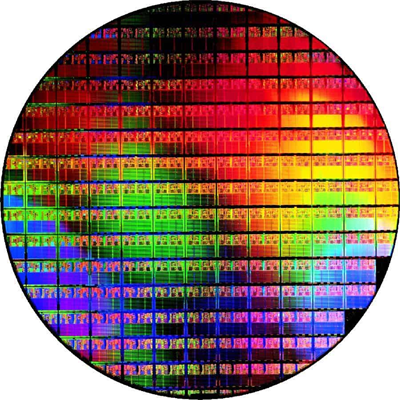
1) Wafer wafer adopts tin gold sheet process, and the cost of materials and equipment is high
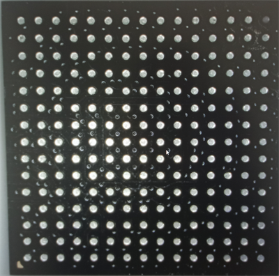
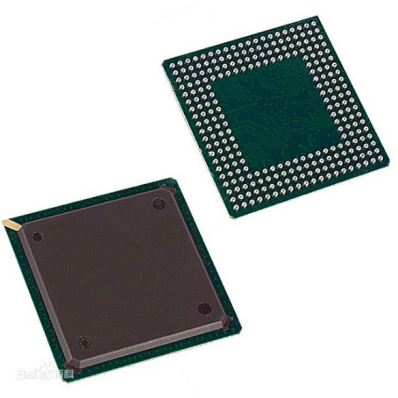
2) BGA traditional stencil, solder paste ball planting process, pollution, multi-stencil
3) Localization of memory chips and equipment
Wafer & BGA
Application Features:
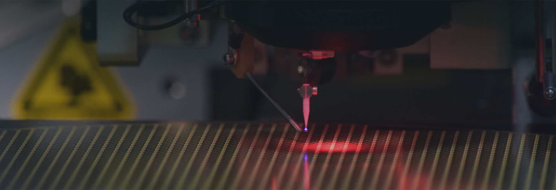
1) Simple laser process, low cost, environmental protection and energy saving
2) No spatter residue, no reflow soldering required
3) Smaller ball diameter operation <100umMemory Chip Application FeaturesLocalization, high efficiency, low cost
Wafer wafer, BGA ball mounting, memory chip:
1. Ball diameter: 0.1mm-0.89mm
2. PITCH diameter: Min =100μm
3. Surface material: gold-plated, tin-plated, silver-plated
4. Soldering space: the center of the pad and the edge of the device ≥ 1mm
5. Device height: up to 10mm from the processing surface to the top surface of the device


Previous page
Next page
Previous page
Next page

